
San Francisco circuits has released an in-depth resource detailing the eight crucial types of Printed Circuit Board (PCB) vias, designed to assist designers, engineers, and procurement teams in overcoming the complexities of contemporary board manufacturing. Discover more > >
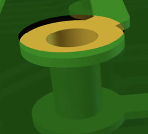
Stacked PCB Via.
As electronic devices become increasingly compact and intricate, the role of Printed Circuit Board vias is vital for facilitating multi-layer connections, maintaining high-speed signal integrity, and enhancing thermal performance.
Exploring the 8 Key Types of PCB Vias
each type of via is tailored to fulfill specific functions based on the board’s architecture, component density, and electrical specifications:
- Through-Hole vias: These are standard, full-depth vias that link all layers of the PCB.
- Blind Vias: These connect the outer layers to selected inner layers without extending through the entire board.
- buried Vias: These are used to connect internal layers only and are not visible from the outer surfaces.
- Microvias: Created through laser drilling (≤150 µm), these are perfect for high-density interconnect (HDI) and compact designs.
- Stacked Vias: These consist of vertically aligned blind or microvias,ideal for dense multi-layer connections.
- Staggered Vias: These are offset vias that help minimize stress and enhance reliability.
- Tented Vias: These are covered with a solder mask for added protection and isolation.
- Via-in-Pad (VIP): Positioned beneath component pads, these are essential for ball grid array (BGA) configurations and thermal management.
The Importance of Vias: Performance, Reliability, and Manufacturability
- Space Efficiency: Implementing blind, buried, or microvias can significantly enhance routing density.
- Heat Management: Utilize thermal vias for effective heat dissipation beneath power components.
- Signal Quality: VIP and staggered vias can definitely help minimize signal path lengths and reduce crosstalk.
- Mechanical Integrity: Through-hole vias provide exceptional structural strength.
Whether your project involves RF applications, HDI boards, or critical systems, understanding the appropriate use of each via type is essential for cost reduction, performance enhancement, and manufacturability assurance.
With extensive experience in producing complex multilayer and HDI PCBs, San Francisco Circuits offers advanced via solutions, including:
- Laser-drilled microvias
- Sequential lamination for stacked and buried vias
- Via-in-pad filling and capping
- Thermal via optimization for components sensitive to heat
Our engineering team is ready to assist in optimizing your stackup and via strategy to meet rigorous performance, size, and reliability standards.
For a detailed overview of the various types of PCB vias, visit the San Francisco Circuits website.


