
San Francisco Circuits (SFC) recognizes that Bluetooth technology is a prevalent wireless solution utilized across various industries, including industrial monitoring, home automation, consumer gadgets, and peripheral devices.Discover more >>
Nevertheless, improper PCB design can lead to issues such as signal interference, restricted range, and data loss—challenges that persist even with advancements in the protocol.
Although Bluetooth 5.0 presents critically important improvements over earlier versions like 4.2, basic wireless limitations—such as relatively low data rates, inadequate wall penetration, and vulnerability to external interference—still necessitate hardware-level solutions.
Tailored Applications and Universal Engineering Principles
in the complete article, SFC discusses how design engineers must consider the specific operational characteristics of their products, whether they are developing a retail beacon, a wireless audio headset, or a smart home device. Each application has unique performance criteria, yet they all benefit from common design principles:
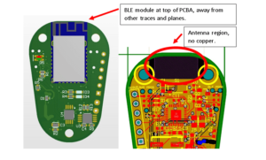
Proper antenna positioning should be distanced from noise sources and integrated within an optimized grounding structure.
Effective power supply filtering is essential for maintaining voltage stability and preventing signal variations.
Careful trace layout and impedance management are vital for ensuring signal integrity and minimizing electromagnetic interference (EMI).
Implementing shielding and separating ground planes can further mitigate noise in environments dense with radio frequencies.
These factors substantially impact signal quality and the overall performance of Bluetooth modules in practical applications.
Advancing Protocols, Ongoing Hardware Requirements
Having been around for over twenty years, Bluetooth technology continues to progress—yet the necessity for RF-aware PCB design remains unchanged. As applications demand greater performance from compact wireless systems, success hinges on optimizing both electrical and physical designs from the outset.
San Francisco Circuits further elaborates on strategies to enhance PCB design for Bluetooth circuit boards, including utilizing certified modules, evaluating Bluetooth device choices, isolating or eliminating copper signals and high-power components, and accounting for real-world obstacles, among other considerations.
Explore the complete article, or visit the SFC website for additional insights.


