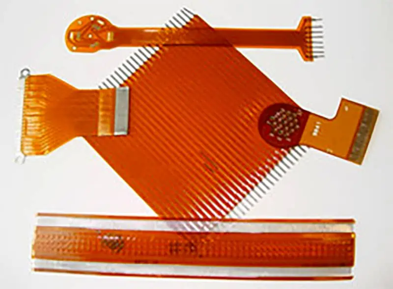
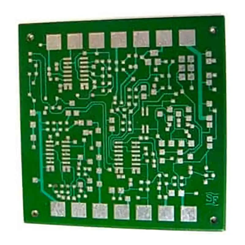
San Francisco Circuits has published an insightful piece that delves into the various aspects of PCB trace widths and layouts, detailing when and how to integrate these elements into PCB designs tailored for specific applications.
For the complete article, visit San Francisco Circuits’ website here.
PCB traces serve as conduits for signals—be it analog,digital,or power—linking different points on the circuit board. In scenarios where design specifications demand enhanced speed, reduced noise, or the management of high current or voltage, selecting the appropriate trace widths and types can take precedence over minimizing the manufacturing costs of the bare PCB or the overall dimensions of the board.
This article explores:
- The definition of trace width and its meaning in PCB design
- Specific trace requirements that may increase PCB manufacturing and testing expenses
- Illustrations of various trace widths and thicknesses
- The methodology for calculating PCB trace width
- The approach to determining PCB trace resistance
- Considerations for trace spacing and length
- The role of ground-filled traces and planes
- Optimal practices for routing PCBs
To gain deeper insights into how trace specifications influence PCB design and to learn how to strike a balance between fabrication costs, circuit density, and overall functionality, check out the full article on San Francisco Circuits’ website.

