San Francisco Circuits has published a comprehensive guide on the 8 most essential types of Printed Circuit Board (PCB) vias, helping designers, engineers, and procurement teams navigate the challenges of modern board manufacturing. Learn more > >
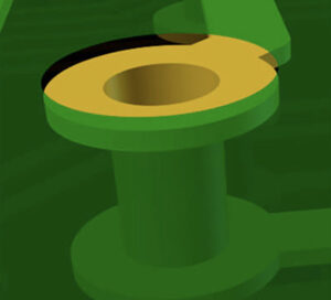
Stacked PCB Via.
As electronic devices continue to shrink in size while increasing in complexity, Printed Circuit Board vias play a critical role in enabling multi-layer interconnections, high-speed signal integrity, and thermal performance.
The 8 Main Types of PCB Vias
Each via type serves a specific function depending on the board’s structure, component density, and electrical requirements:
- Through-Hole Vias: Standard, full-depth vias that connect all PCB layers.
- Blind Vias: Connect outer layers to select inner layers without penetrating the entire board.
- Buried Vias: Connect internal layers only; invisible from the outer surfaces.
- Microvias: Laser-drilled vias (≤150 µm), ideal for HDI and miniaturized designs.
- Stacked Vias: Vertically aligned blind/microvias for dense multi-layer connections.
- Staggered Vias: Offset vias that reduce stress and improve reliability.
- Tented Vias: Covered with solder mask for protection and isolation.
- Via-in-Pad (VIP): Placed beneath component pads, critical for BGA and thermal performance.
Why it Matters: Performance, Reliability & Manufacturability
- Space Optimization: Use blind, buried, or microvias to increase routing density.
- Thermal Management: Leverage thermal vias for heat dissipation beneath power devices.
- Signal Integrity: Reduce signal path lengths and crosstalk with VIP and staggered vias.
- Structural Strength: Through-hole vias offer excellent mechanical robustness.
Whether you’re building for RF applications, HDI boards, or mission-critical systems, knowing when and how to use each via type is key to reducing cost, improving performance, and ensuring manufacturability.
With expertise in fabricating complex multilayer and HDI PCBs, San Francisco Circuits offers advanced via capabilities, including:
- Laser-drilled microvias
- Sequential lamination for stacked & buried vias
- Via-in-pad filling and capping
- Thermal via optimization for heat-sensitive components
Our engineering team can help optimize your stackup and via strategy to meet stringent performance, size, and reliability requirements.
Read more including the full breakdown on the Types of PCB vias on the San Francisco Circuits website.

