San Francisco Circuits (SFC) understands that Bluetooth remains a widely adopted wireless solution across sectors ranging from industrial sensing and home automation to consumer electronics and peripheral devices. Find out more >>
However, without careful PCB design, Bluetooth implementations are prone to signal interference, limited range, and data loss—issues that persist despite recent improvements in the protocol.
While Bluetooth 5.0 offers notable gains over previous iterations such as 4.2, the core wireless characteristics—relatively low throughput, poor wall penetration, and susceptibility to external noise—still demand mitigation at the hardware level.
Application-Specific Demands, Common Engineering Principles
In the full article, SFC touches on how design engineers must account for the unique operational profile of their product, whether it’s a retail beacon, a remote audio headset, or a smart home device. Each use case presents distinct performance requirements, but all benefit from shared design fundamentals:
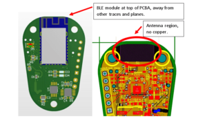
Antenna placement must be isolated from noise sources and enclosed within an optimised ground structure.
Power supply filtering ensures voltage stability to avoid signal fluctuations.
Trace layout and impedance control are critical for preserving signal fidelity and minimising EMI.
Shielding and ground plane separation can further reduce noise in RF-dense environments.
These considerations directly influence signal quality and overall Bluetooth module effectiveness in real-world deployments.
 Evolving Protocols, Persistent Hardware Needs
Now more than two decades old, Bluetooth continues to evolve—yet the importance of RF-conscious PCB design remains constant. As applications demand more from smaller wireless platforms, success depends on optimising the electrical and physical design from the start.
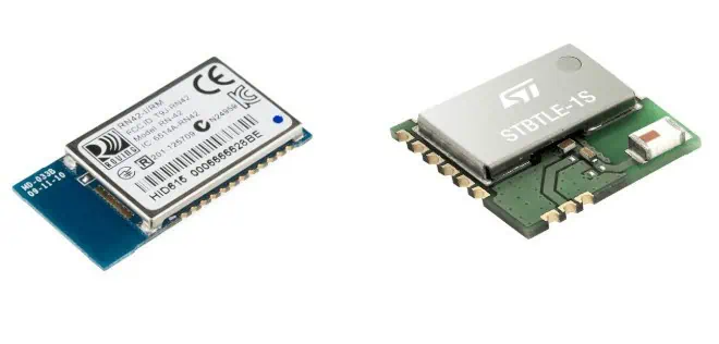
San Francisco Circuits goes on to explore how to improve PCB design for bluetooth circuit boards, such as by using certified modules, checking Bluetooth device selection, separating or removing copper signals and high-energy components, considering real-world obstructions, and more.
Read the full article, or visit the SFC website to find out more.


