Maximizing Space Efficiency in PCB Designs with Pogo Pin Interfaces
San Francisco Circuits has published an insightful piece discussing the advantages of utilizing pogo pin interfaces to optimize space in SWaP (size, weight, and power)-sensitive printed circuit board (PCB) designs. This is notably relevant for compact applications such as drones, unmanned vehicles, and various robotic systems.
The Challenge of Conventional Programming Connectors
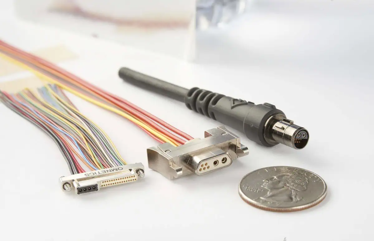
Typically, embedded firmware is uploaded to a circuit board via a programming connector, which can be cumbersome and occupy essential real estate on the board. Additionally, these connectors frequently enough come with a higher price tag compared to other components.
Innovative Solutions with Pogo Pins
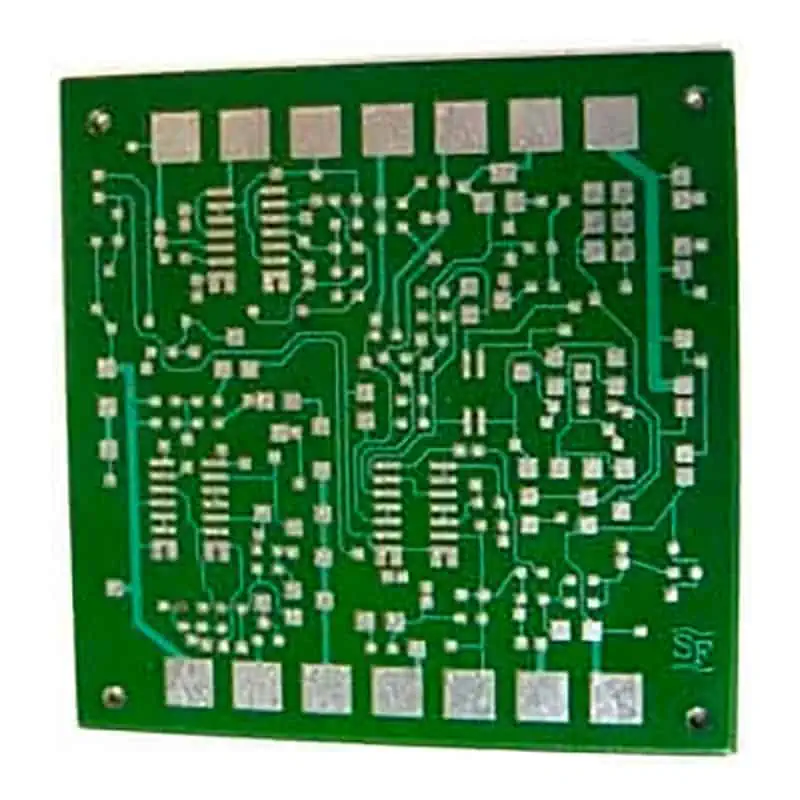
In many scenarios, these traditional connectors can be substituted with a series of exposed copper pads.By employing pogo pins—spring-loaded contacts that can be easily attached or held in place—designers can transition from bulky header connections to sleek, low-profile alternatives. This shift not only conserves valuable board space but also reduces costs substantially.
Real-world Applications and Benefits
the article elaborates on various practical applications of pogo pin connection interfaces in PCBs, highlighting their role in facilitating faster and more reliable testing and debugging processes. For those interested in exploring this innovative approach further,the complete article is available on the San Francisco Circuits website.

