San Francisco Circuits emphasizes the vital importance of Printed Circuit Board (PCB) stack-ups in enhancing reliability, performance, and cost-effectiveness. This article delves into essential factors, cutting-edge technologies, and optimal practices to assist engineers in refining designs for a variety of applications, ranging from high-frequency RF boards to flexible circuits. Discover more > >
In the realm of PCB design, the importance of stack-up configuration is frequently overlooked. Nevertheless, a meticulously designed stack-up can profoundly influence reliability, performance, and overall cost efficiency. Inadequately defined stack-ups—characterized by missing data, erroneous parameters, or overly generalized assumptions—can result in manufacturing difficulties and heightened costs.
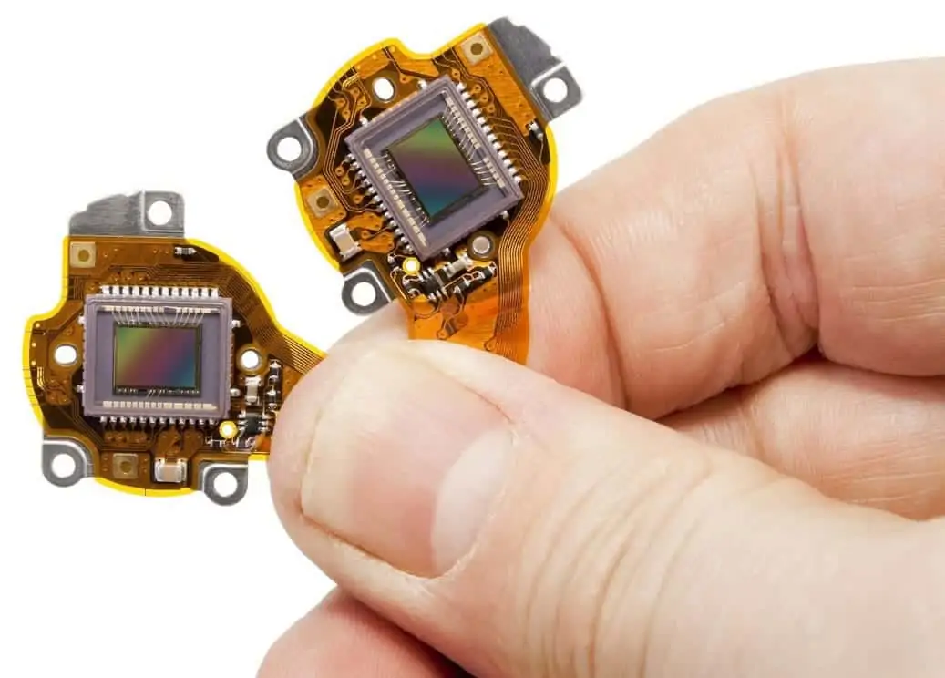
A PCB stack-up delineates the arrangement of conductive and insulating layers, which directly affects signal integrity, power distribution, and susceptibility to electromagnetic interference. Whether dealing with multi-layer PCBs, metal-core configurations, or high-density interconnects (HDIs), each variant necessitates thorough consideration. Advanced applications, such as high-frequency RF boards and flexible circuits used in wearable technology, present distinct stack-up requirements that influence aspects like thermal management and mechanical resilience.
Several key elements influence PCB stack-ups, including component density, lamination techniques, mechanical limitations, and electrical performance criteria. Engineers face critical choices, such as selecting between foil and cap construction, optimizing ground planes, and ensuring accurate impedance control.
Grasping these complexities is essential for achieving peak performance and manufacturability.
Visit the San Francisco Circuits website to read the complete article and gain expert insights into PCB stack-ups, recommended practices, and industry standards.

